A handful of nice precision components engineering pictures I located:
At perform in a shipyard joiners’ shop
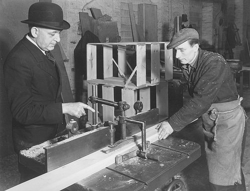
Image by Tyne & Put on Archives & Museums
A scene from the Joiner’s shop of a Sunderland shipyard, probably that of Sir James Laing & Sons, January 1948, (TWAM ref. DS.JLT/5/four/two/5).
Sunderland has a remarkable history of innovation in shipbuilding and marine engineering. From the development of turret ships in the 1890s and the production of Doxford opposed piston engines following the Very first World War via to the designs for Liberty ships in the 1940s and SD14s in the 1960s. Sunderland has significantly to be proud of.
Tyne & Wear Archives cares for tens of thousands of photographs in its shipbuilding collections. Most of these concentrate on the ships – in distinct their construction, launch and sea trials. This set looks to redress the balance and to celebrate the operate of the guys and women who have played such a essential element in the region’s history. The images show the human side of this excellent story, with a lot of relating to the world famous shipbuilding and engineering firm William Doxford & Sons Ltd.
The Archives has created a brief weblog to accompany these photos.
(Copyright) We’re satisfied for you to share these digital photos inside the spirit of The Commons. Please cite ‘Tyne & Put on Archives & Museums’ when reusing. Specific restrictions on higher quality reproductions and industrial use of the original physical version apply although if you are unsure please email archives@twmuseums.org.uk
Not your usual SPARC
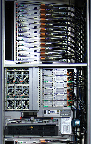
Image by nhr
Spotted at a new datacenter: an interesting, custom SPARC-primarily based computing program for really huge scientific workloads — this rack is component of a computer cluster that can solve a system of linear equations with far more than ten million variables.
Each SPARC CPU is a 8-core chip clocked at 2GHz, and every single core has 256 (!) double precision floating-point registers and 4 multiply-add units. That quantity of FP registers is adequate to compute a 8×8 matrix multiplication with no requiring any access to RAM beyond the initial loading and final storing of the FP data. Accesses to the "slow" L1, L2 caches and RAM are as a result minimized, allowing the CPU to crunch numbers at higher speed.
Operations on massive matrixes can be effectively divided e.g. into 8×8 block decompositions that match in the register file.
Every multiply-add unit can output on each clock cycle the result of an operation of the kind D := A * B + C exactly where A, B and C are double precision FP numbers.
The SPARC CPU’s maximum FP throughput is thus 2GHz * eight cores * four fused mutiply-adds = 128 GFLOPs/CPU. Each SPARC CPU has a memory bandwidth of 64GBytes/s.
A SPARC CPU, together with 16GB of RAM and an Interconnect Controller (ICC), form a unified "compute node".
The ICC combines, on a single VLSI, 4 5GBytes/s DMA interfaces and a crossbar switch / router with ten 5GBytes/s bidirectional links. These ten links connect to other compute nodes, forming a virtual 6D fused torus / mesh network structure.
Compute nodes can access the memory of other nodes making use of virtual addressing, as a remote DMA operation. The ICC of the destination node performs the needed virtual to physical address translation and the actual DMA. The ICC can also perform easy arithmetic operations on integers and FP data, enabling the parallel computation by the communication fabric itself of barrier operations, without obtaining to involve the SPARC CPU.
Four compute nodes are integrated on each system board, and each rack holds 24 hot swappable program boards.
The image shows the upper twelve technique boards in a rack. Also visible are the nine air-cooled, redundant power supply units, the six I/O controller units, as effectively as two blade-like, redundant rack supervisor controllers and a Fujitsu storage array containing the operating technique boot disks.
The six I/O controller units are water-cooled, and every single includes a single unified compute node. These I/O controllers connect the rack to other racks and to a high-speed clustered local storage program with a capacity of about 11 petabytes, and a international file system of about 30 PBytes. The operating system of the unified compute nodes is a custom fault-resilient multi-core Linux kernel the mass storage technique is primarily based on Lustre.
The peak FP functionality of each rack is 128 GFLOPs/compute node * (4 compute nodes / method board * 24 technique boards + 6 I/O controller compute nodes ) / rack = 128GFLOPs * (four*24+6) = 13056 GFLOPs, or 13.056 TeraFLOPs the total memory size per rack is 1632 Gigabytes.
Every single rack requires about 10KW of electrical energy, and the higher-speed 6D torus inter-node connection fabric has been developed to efficiently extend to hundreds of such racks. Beware that electricity bill…
In this information center, a cluster of 864 of these racks kind a huge parallel supercomputer, with 1400 Terabytes of RAM, and a theoretical peak FP overall performance of 13.056 TFLOPs * 864 = 11.280 PetaFLOPs — i.e. more than eleven million gigaFLOPs.
The powerful LINPACK performance is about 93% of that theoretical peak.
The major intended application area seems to be the life sciences, with an emphasis on molecular modelling ab initio — simulating complete molecules starting from the quantum behavior of elementary nucleons and electrons — to assist the design of new drugs, simulate biochemical processes like chemotherapy agent resistance of cancer cells at the molecular level, model neural processes and so on.
Climate modelling, atomic level simulation of novel nanomaterials and computational fluid dynamics applications are also in the input queue.